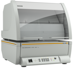
Universal instrument for automated measurements on smallest structures, multilayers, functional coatings and very thin coatings < 0.1 µm
Microfocus tube with tungsten anode; molybdenum anode optional
Measuring direction with measuring top down
4-fold changeable filters
Polycapillary optics permit particularly small measuring spots Ø approx. 20 or 10 µm
Silicon drift detector 20 or 50 mm² for highest precision on thin layers
Programmable measuring table for printed circuit boards up to 613 × 610 mm, optionally with vacuum function
Applications
Au/Pd/Ni/CuFe and Sn/Ni coatings in the micro- and nanometer range
Assembled and unassembled circuit boards
Testing of base metallization layers (under-bump metallization, UBM) in the nanometer range
Measurement of light elements, e.g. determination of the phosphorus content (in ENEIG/ENEPIG) under Au and Pd
Lead-free solder caps on copper pillars
Testing the elemental composition of C4 and smaller solder bumps, as well as small contact surfaces in the semiconductor industry
Brochure