Automated Optical Inspection (AOI)
In electronics and semiconductor-related production, inspection speed means very little without repeatability and useful defect data. That is why Automated Optical Inspection (AOI) systems are widely used to verify assembly quality, detect placement and solder issues early, and support tighter process control across inline and batch environments.
On this page, you can explore AOI solutions for different inspection tasks, from SMT and PCBA verification to coating inspection and metrology-oriented applications. The range includes systems suited to high-mix manufacturing, production lines that require fast programming, and inspection workflows where traceability, barcode reading, OCR, and defect review all matter.
Where AOI fits in the inspection workflow
AOI is used to inspect boards, components, packages, and assembled products by combining cameras, optics, lighting, motion control, and software algorithms. In practice, it helps identify visible defects such as missing parts, polarity errors, skew, lifted leads, solder bridging, contamination, and marking inconsistencies before products move to later stages of test or shipment.
Within a broader quality strategy, AOI often works alongside other inspection and validation methods. For applications that require a wider view of wafer- and package-level quality control, it can be helpful to also review semiconductor defect inspection equipment depending on the type of defects being targeted.
Common AOI system types in this category
This category includes both inline AOI and batch-style inspection platforms. Inline systems are typically selected for continuous production flow, where boards move through the line with standard communication interfaces and inspection results must be available quickly for rework or process correction. Batch AOI is often preferred for offline verification, engineering review, lower-volume production, or applications where operators need more flexibility around loading and programming.
There are also systems oriented toward specific inspection goals. Some are designed for conventional SMT and solder-joint verification, while others focus on coatings, dispensed material coverage, or higher-accuracy measurement tasks. If you are comparing solutions beyond this semiconductor-focused category structure, you may also want to browse the broader AOI equipment range available here.
Representative systems and practical use cases
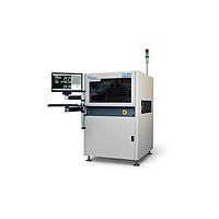
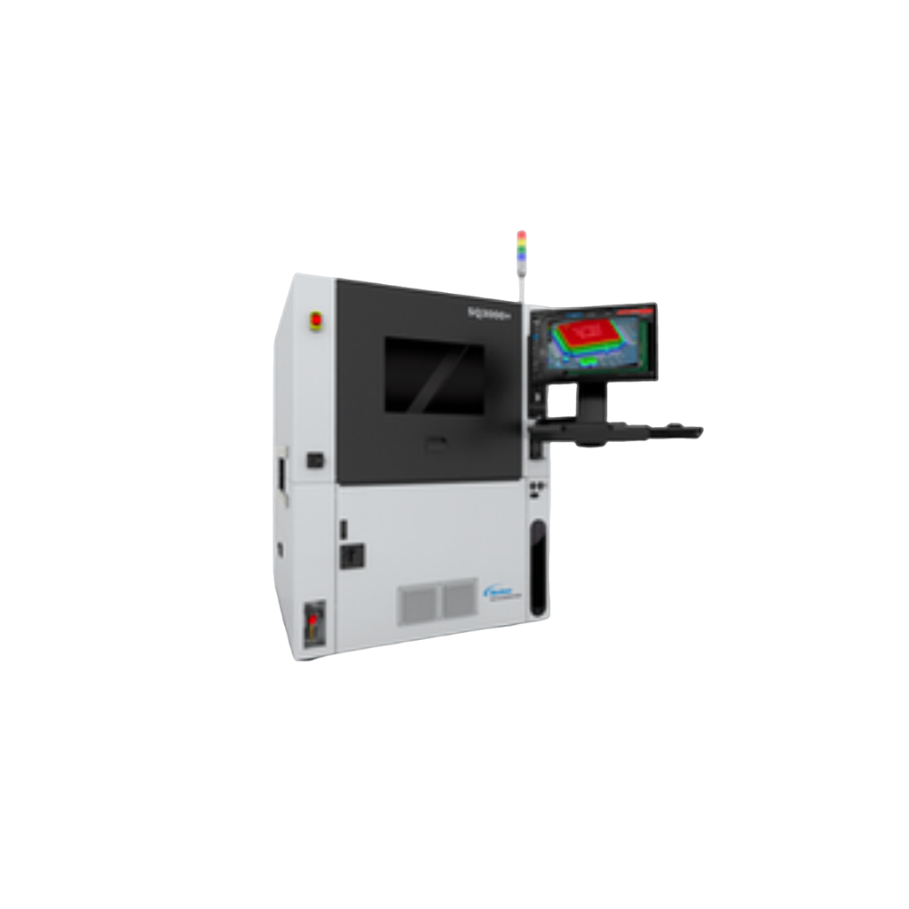
Among the featured options, Nordson appears with several systems covering different inspection needs. The Nordson SQ3000+ Automated Optical Inspection and the Nordson SQ3000M2 Automated Optical Inspection and Metrology System are relevant for users who need not only defect detection but also more advanced measurement capability, support for a broad range of package types, and compatibility with production data workflows such as CAD-based programming and SPC-oriented review.
For conformal coating and dispensed material inspection, the Nordson AOI FX-940UV In-Line Optical Inspection is positioned around coverage verification, crack detection, and delamination-related checks. This makes it useful where standard component presence inspection is not the only concern and UV-based inspection support improves visibility of coating quality.
Maker-Ray adds practical options for inline PCBA inspection, including the AIS300, AIS301, and AIS 501 platforms, as well as AIS203 variants intended for DIP component inspection. These systems are relevant for manufacturers looking at board size compatibility, OCR or barcode reading, and image-based inspection in production settings where communication through SMEMA and straightforward software functions are part of the requirement.
For offline or batch inspection, the MANNCORP Sherlock-300B Batch AOI Machine is an example of a solution used where loading flexibility, CAD conversion, offline programming, and operator-guided review are important. This type of setup can make sense in NPI, repair support, or lower-volume production where an inline conveyor is not essential.
What to consider when selecting an AOI machine
The right platform depends first on the product being inspected. Board size range, component height clearance, supported package types, and the defects you need to catch should be checked before comparing software features. A line focused on fine-pitch SMT, BGAs, and polarity verification may prioritize different optics and lighting behavior than a process focused on DIP assemblies or conformal coating coverage.
It is also important to evaluate inspection resolution, field of view, and whether the system provides only image-based inspection or includes 3D or metrology-oriented functions. For example, some systems in this category emphasize coplanarity, lifted lead detection, and height-related measurement, while others focus on faster rule-based and image comparison workflows for common assembly defects.
Programming time and usability are equally important in high-mix manufacturing. Systems that support OCR, barcode reading, CAD import, or training tools can reduce changeover effort and help engineering teams manage frequent model changes more efficiently.
Key technical features that affect inspection performance
AOI performance is shaped by the interaction between optics, camera resolution, lighting design, motion system accuracy, and software algorithms. Multi-angle lighting, coaxial illumination, UV lighting, and high-resolution color imaging each serve different purposes depending on whether the target is solder quality, component shape, package marking, or coating visibility.
On the software side, functions such as OCR, OCV, barcode recognition, rule-based inspection, image comparison, and AI-assisted interpretation can improve inspection coverage and reduce manual review time when properly configured. In environments where process tracking and yield analysis matter, SPC and defect review tools can also help transform AOI from a simple gatekeeper into a more complete process control resource.
AOI in semiconductor and electronics manufacturing environments
Although many systems in this category are directly relevant to PCBA inspection, AOI also plays a role in semiconductor-adjacent manufacturing where package integrity, device orientation, contamination, wire-related defects, and marking verification must be controlled. This is especially relevant when inspection has to support traceability and consistent quality checks across multiple product formats.
In some production cells, AOI is only one part of a more stable inspection environment. Supporting equipment such as industrial chillers for inspection systems may be considered where thermal stability is important for equipment performance or surrounding process conditions.
How to compare suppliers and product families
When comparing product families, it helps to look beyond headline speed and ask how each machine fits your actual workflow. Inline communication, supported PCB dimensions, defect libraries, software training tools, review capability, rework integration, and maintenance practicality can have more impact on day-to-day results than a single throughput figure.
It is also useful to compare whether a supplier offers multiple models for different inspection stages. In this category, Nordson and Maker-Ray illustrate two different kinds of portfolio depth: one with options spanning AOI, metrology, and coating inspection, and another with several inline PCBA and DIP-focused configurations. That kind of range can matter if you expect your inspection requirements to expand over time.
Choosing the right AOI setup for your production goals
A suitable AOI system should align with your assembly type, target defects, throughput expectations, and data requirements. Whether you need compact batch inspection, inline solder-joint verification, coating inspection, or a platform with stronger metrology capability, the best choice is usually the one that balances detection reliability with manageable programming and operation.
Use this category to compare available AOI equipment by application focus, inspection method, and production fit. If your process also depends on broader semiconductor inspection or environmental support equipment, the related categories above can help you build a more complete inspection and quality-control workflow.
Get exclusive volume discounts, bulk pricing updates, and new product alerts delivered directly to your inbox.
By subscribing, you agree to our Terms of Service and Privacy Policy.
Direct access to our certified experts