
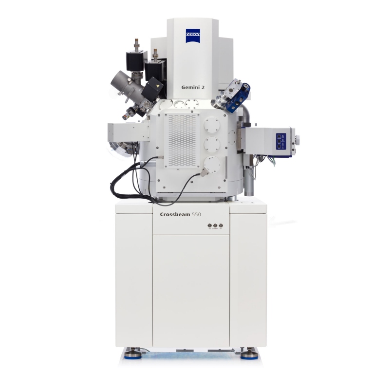
ZEISS Crossbeam 550 Electron Microscopy
SEM Schottky Emitter:
1.4 nm @ 1 kV
1.2 nm @ 1 kV with Tandem decel
1.6 nm @ 200 V with Tandem decel
0.7 nm @ 15 kV
0.6 nm @ 30 kV (STEM mode)
1.8 nm @ 1 kV (WD 5 mm)
1.3 nm @ 1 kV with Tandem decel (WD 5 mm)
0.9 nm @ 15kV (WD 5 mm)
2.3 nm @20 kV & 10 nA (WD 5 mm)
Beam current: 10 pA – 100 nA
Store Resolution: 32 k × 24 k (up to 50 k × 40 k with optional Atlas 5 3D Tomography module)
Detection Limit: < 4,2 ppm boron in silicon
Lateral Resolution: < 35 nm
Mass/Charge Range: 1-500 Th
Mass Resolution: m/Δm > 500 FWTM
Depth Resolution: < 20nm AlAs/GaAs multilayer system
Get exclusive volume discounts, bulk pricing updates, and new product alerts delivered directly to your inbox.
By subscribing, you agree to our Terms of Service and Privacy Policy.
Direct access to our certified experts